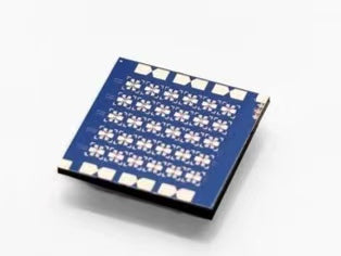
NANO PRO™ GFET Sensor Chip (Back-Gate, EOT = 5nm)
NANO PRO™ provide GFET Sensor Chip for Measurements in Liquid Medium. The chip provides 30 backgated graphene devices distributed in a grid pattern on the chip. All the 30 devices have a 3-probe geometry, provide a backgate with an EOT = 5nm. This scheme allows for individual control of the conductance of each of the graphene channels within the die. There are 3 graphene channel dimensions to allow investigation of size dependence on device properties, enabling immediate optimization.
Typical Specifications
- Growth method: CVD synthesis
- Graphene transfer: Polymer assisted transfer
- Chip dimensions: 10 mm x 10 mm
- Chip thickness: 525 μm
- Number of channels per chip: 30
- Gate oxide thickness (EOT): 5 nm
- Gate oxide material: Al2O3
- Dielectric breakdown: >13kV/mm
- Metallization: Au Contacts
- Graphene field-effect mobility: > 600 cm2/V.s
- Dirac point:
- Optical Yield: ≥ 75 %
Absolute Maximum Ratings
-
Maximum gate-source voltage: ± 5 V
- Maximum temperature rating: 150 °C
- Maximum drain-source current density: 107A.cm-2
Quality Control
All our samples are subjected to a rigorous QC in order to ensure a high quality products.
- Optical microscopy inspection of all the devices
- Raman Spectroscopy of each fabrication batch
- Electrical characterization via back gating of each fabrication batch
Applications
Graphene field-effect transistors (GFETs) have unprecedented sensitivity to the surrounding environment and is an ideal transducer for a variety of sensing applications. Depending on the application, GFETs can be tuned to be sensitive only to the stimulus of interest and have shown breakthrough performance in areas such as graphene device research, chemical sensing, bioelectronics and biosensing.